
From Vacuum Tubes to Solid State
Every electronic circuit is built from devices that give a controlled flow of electrons. Before the transistor (1948), that meant vacuum tubes (valves): the vacuum diode (anode/plate + cathode), triode (+ grid), tetrode and pentode. A heated cathode supplied electrons; voltages between electrodes controlled their flow through vacuum (needed so electrons don't lose energy colliding with air molecules). Current flows only cathode → anode — one way, hence 'valves'.
Their problems: bulky, high power consumption, high voltages (~100 V), limited life, low reliability.
The 1930s realisation: some solid-state semiconductors and their junctions let you control the number and direction of charge carriers — with light, heat or small voltages changing the number of mobile charges. The advantages invert every vacuum-tube weakness:
| Vacuum tubes | Semiconductor devices |
|---|---|
| electrons from heated cathode | charge carriers generated within the solid |
| evacuated inter-electrode space | no vacuum needed |
| bulky, ~100 V, power-hungry | small, low voltage, low power |
| short life, unreliable | long life, high reliability |
(Historical gem: a natural galena (PbS) crystal with a metal point contact served as a radio-wave detector before semiconductor physics was even understood.)
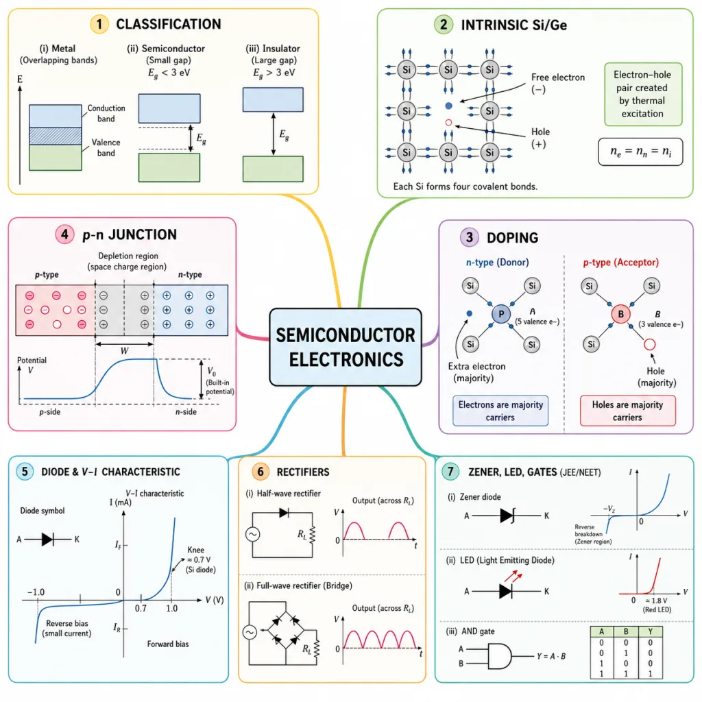
Classification I: By Conductivity
On the basis of resistivity (or conductivity ):
| Class | Resistivity (ohm m) | Conductivity (S/m) |
|---|---|---|
| Metals | - | - |
| Semiconductors | - | - |
| Insulators | - | - |
(The values are indicative; resistivity alone is not the full story — the band picture below completes it.)
The semiconductor family
- Elemental: Si and Ge — the workhorses.
- Compound inorganic: CdS, GaAs, CdSe, InP…
- Organic: anthracene, doped phthalocyanines; organic polymers: polypyrrole, polyaniline, polythiophene — the seeds of polymer/molecular electronics (post-1990).
This chapter concentrates on Si and Ge; the concepts transfer to compound semiconductors.
[NEET Important] The resistivity ranges are direct one-markers. Anchor: metals below , insulators above , semiconductors in the vast middle.
Classification II: By Energy Bands
In an isolated atom, electron energies are sharp Bohr levels. In a solid, atoms sit so close that outer orbitals overlap; each of the ~ electrons sees a slightly different charge environment and takes a slightly different energy. The levels smear into energy bands:
- Valence band (VB): the band of valence-electron energies — highest level .
- Conduction band (CB): the band above — lowest level .
- Energy band gap: , which may be large, small or zero.
The Si/Ge counting argument
A crystal of N atoms of Si (outer orbit n = 3) or Ge (n = 4) has 4N valence electrons but 8N available outer states (2s + 6p). At crystal spacing, these 8N states split into two bands of 4N states each, separated by : at absolute zero the lower (valence) band is completely full, the upper (conduction) band completely empty.
The three cases (NCERT Fig. 14.2)
- Metals: CB and VB overlap (or the conduction band is partially filled) — electrons move freely; huge conductivity.
- Insulators: large gap, > 3 eV — thermal excitation cannot lift electrons across; CB stays empty; no conduction.
- Semiconductors: small gap, < 3 eV — at room temperature some electrons cross into the CB (leaving useful vacancies behind); modest conductivity.
The group-IV ladder — memorise
| Element | Verdict | |
|---|---|---|
| C (diamond) | 5.4 eV | insulator |
| Si | 1.1 eV | semiconductor |
| Ge | 0.7 eV | semiconductor |
| Sn | 0 eV | metal |
Same column of the periodic table, four different electrical fates — the band gap decides everything.
[JEE Tip] Band edges , drawn as lines are space-averaged levels (Points to Ponder) — bottom-of-CB and top-of-VB, not locations in the crystal. And the ordering is NCERT Exercise 14.3's answer — asked constantly.
Solved Examples
Example 1: Why is C insulating but Si and Ge semiconducting? (NCERT Example 14.1)
Carbon, silicon and germanium share the same lattice structure. Explain the different behaviour.
Solution:
- The four bonding electrons sit in the 2nd orbit (C), 3rd (Si), 4th (Ge).
- The farther the orbit, the smaller the energy needed to free an electron: ionisation is hardest for C, easier for Si, easiest for Ge — mirrored in : 5.4, 1.1, 0.7 eV.
- So free-electron numbers at room temperature are negligible in C but significant in Si and Ge.
- Takeaway: identical structure, different orbit radius → different band gap → insulator vs semiconductor.
Example 2: Classify by resistivity [Board Rapid]
Materials A, B, C have resistivities , and ohm m. Classify them.
Solution:
- A: ohm m — within -: metal.
- B: — within -: semiconductor.
- C: — within -: insulator.
- Takeaway: slot the exponent into the three ranges; boundaries are approximate but exam values sit safely inside.
Example 3: The 4N/8N band split [Board Conceptual]
A silicon crystal has N atoms. Account for the filling of its two outer bands at absolute zero.
Solution:
- Each Si atom offers 4 valence electrons → 4N electrons; the outer orbit could hold 8 per atom → 8N states.
- At crystal spacing the 8N states split into two bands of 4N states each, gap between.
- At 0 K the 4N electrons exactly fill the lower band: valence band full, conduction band empty.
- Takeaway: a full band conducts nothing (no empty states to move into) — which is why pure Si at 0 K is an insulator.
Example 4: Metal without overlap [Conceptual]
NCERT says a metal arises with overlapping bands OR a partially filled conduction band. Why does partial filling alone guarantee conduction?
Solution:
- Conduction requires electrons to gain energy from a field, i.e. to move into nearby empty states.
- In a partially filled band, empty levels sit immediately above filled ones — electrons accelerate freely.
- In a full band there is nowhere to go (Pauli); in an overlap, VB electrons spill into CB states — same effect.
- Takeaway: 'empty states adjacent to filled states' is the true criterion for metallic conduction.
Example 5: Thermal test of an insulator [NEET Numerical]
Estimate why room-temperature thermal energy cannot make diamond conduct. (kT at 300 K ≈ 0.026 eV.)
Solution:
- Diamond's gap: = 5.4 eV; thermal quantum: ~0.026 eV.
- Ratio: — excitation probability ~ is vanishingly small.
- Conclusion: effectively zero electrons reach the CB — insulator. For Si (1.1 eV ≈ 42 kT) the exponential is tiny but nonzero: a weak semiconductor.
- Takeaway: conduction is an exponential game in — small gap changes make astronomical carrier differences.
Example 6: Photon threshold of a band gap [JEE Numerical]
What maximum wavelength of light can excite an electron across silicon's 1.1 eV gap?
Solution:
- Condition: photon energy ≥ : .
- Solve: nm.
- Answer: ~1100 nm (near infrared) — silicon absorbs visible light easily, which is why it makes solar cells.
- Takeaway: nm — the bridge between this chapter and photon physics; appears in photodiode/LED problems too.
Example 7: Sn, the group-IV metal [Conceptual]
Tin sits below germanium in group IV yet is a metal. Reconcile this with the band picture.
Solution:
- Down the group the valence orbit moves outward: C(2) → Si(3) → Ge(4) → Sn(5).
- The band gap shrinks correspondingly: 5.4 → 1.1 → 0.7 → 0 eV.
- Zero gap means valence and conduction bands touch/overlap — Sn conducts like a metal.
- Takeaway: one periodic-table column spans insulator → semiconductors → metal purely through .
Example 8: Vacuum-tube vs semiconductor checklist [Board Rapid]
List four advantages of semiconductor devices over vacuum tubes.
Solution:
- Small size and no evacuated bulb or heated cathode (carriers generated within the solid).
- Low operating voltage and low power consumption (tubes needed ~100 V).
- Long life and high reliability.
- Takeaway: NCERT's contrast list verbatim — plus the flexibility that light/heat/small voltages can control carrier numbers, impossible in a vacuum tube.
Example 9: Ordering the gaps (NCERT Exercise 14.3)
C, Si and Ge each have four valence electrons, with gaps , , . Which ordering is true?
Solution:
- Values: C 5.4 eV, Si 1.1 eV, Ge 0.7 eV.
- Ordering: .
- Physical reason: bonding electrons in the 2nd, 3rd, 4th orbits respectively — the more distant, the easier to liberate.
- Takeaway: the exact NCERT exercise answer, recycled endlessly by Boards and NEET.
Example 10: Where do organic semiconductors fit? [Conceptual]
Name the categories of semiconductors with examples, and the technology signalled by polymer semiconductors.
Solution:
- Elemental: Si, Ge.
- Compound inorganic: CdS, GaAs, CdSe, InP.
- Organic: anthracene, doped phthalocyanines; organic polymers: polypyrrole, polyaniline, polythiophene.
- Post-1990 devices from these signal polymer electronics and molecular electronics — NCERT's phrase for the flexible-display future.
- Takeaway: the classification list is a straight recall question; GaAs is the most-quoted compound example.