
Doping: The Conductivity Multiplier
Intrinsic conductivity is too feeble for devices. The fix: add a few parts per million (ppm) of a suitable impurity and the conductivity multiplies enormously. The result is an extrinsic (doped) semiconductor; the deliberate addition is doping, the impurity atoms are dopants.
The size rule: the dopant must not distort the lattice — its atoms must be nearly the same size as Si/Ge, occupying only a few original lattice sites. Hence dopants come from the neighbouring columns of group-IV Si/Ge:
- Pentavalent (valency 5): Arsenic (As), Antimony (Sb), Phosphorus (P) — donors.
- Trivalent (valency 3): Indium (In), Boron (B), Aluminium (Al) — acceptors.
Two different dopant families → two entirely different semiconductor types.
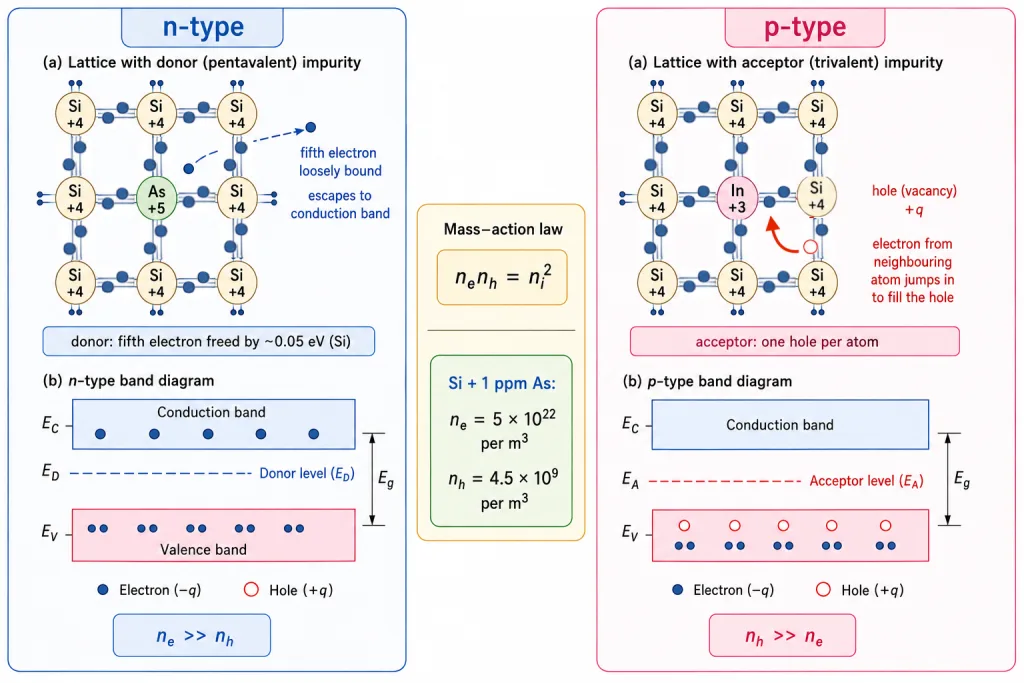
n-type: The Electron Donors
Put a pentavalent atom in a Si site: four of its five valence electrons bond with the four Si neighbours; the fifth is only weakly bound (the bonding four screen the core). Freeing it costs merely ~0.01 eV in Ge, ~0.05 eV in Si — compare the full gap of 0.72 eV (Ge) / 1.1 eV (Si). At room temperature that fifth electron is free.
- Each dopant donates one conduction electron → donor impurity.
- Donated electrons depend on doping level, not temperature; intrinsic generation adds a weak temperature-dependent trickle (with equal holes).
- Extra electrons speed up recombination of holes → hole population falls below .
Result: electrons majority, holes minority —
p-type: The Hole Makers
Put a trivalent atom in: it bonds with only three neighbours; the fourth bond has a vacancy — a hole. A neighbouring bound electron can jump in, moving the hole outward: one acceptor atom yields one conduction hole (and becomes an effectively negative fixed core when it captures that fourth electron).
Result: holes majority, electrons minority —
Key Point: The crystal stays electrically neutral overall — the mobile carriers' charge is exactly balanced by the immobile ionised dopant cores. And in BOTH types, the abundant majority carriers accelerate recombination of the minority ones: doping indirectly suppresses minority carriers below .
Energy Levels of Dopants & the Mass-Action Law
Doping adds new energy states in the gap:
- n-type: donor level sits slightly below — electrons hop from into the conduction band with the tiniest energy supply. At room temperature most donors are ionised while only ~ Si atoms are (per the intrinsic trickle) — so CB electrons come overwhelmingly from donors.
- p-type: acceptor level sits slightly above — valence electrons easily jump up to (equivalently, holes from 'sink' into the valence band; remember: electrons rise, holes sink when given energy). Most acceptors ionise at room temperature.
The law that rules all doping
In thermal equilibrium, whatever the doping:
Raise one carrier type and the other must fall in exact proportion — the quantitative form of minority-carrier suppression.
NCERT Example 14.2 — the canonical calculation
Pure Si: atoms/m³, doped 1 ppm with As; m⁻³.
- Donors: m⁻³. Since this dwarfs : m⁻³.
- Mass action: m⁻³.
One ppm of dopant boosted electrons a million-fold over and crushed holes by nearly seven orders of magnitude.
[JEE Tip] The mass-action division is the chapter's most-set numerical — recognise Example 14.2's numbers on sight. [NEET Important] Level positions: just below (n-type); just above (p-type) — swapping them is the classic wrong option.
Solved Examples
Example 1: The canonical doping calculation (NCERT Example 14.2)
Pure Si ( atoms/m³) is doped with 1 ppm pentavalent As. Find and ( m⁻³).
Solution:
- Donor density: m⁻³.
- Electrons: thermal contribution (~) is negligible beside : m⁻³.
- Holes (mass action): m⁻³.
- Takeaway: majority set by doping; minority set by — the two-step template of every such numerical.
Example 2: Classify the dopants [Board Rapid]
Classify as donor or acceptor for Si: As, B, P, In, Sb, Al.
Solution:
- Donors (pentavalent): As, P, Sb — give n-type.
- Acceptors (trivalent): B, In, Al — give p-type.
- Takeaway: memory hook — donors from group 15 ('Pentavalent Antimony-Arsenic-Phosphorus'), acceptors from group 13 ('Boron-Aluminium-Indium').
Example 3: Why the fifth electron is nearly free [Board Conceptual]
Explain why freeing the pentavalent dopant's fifth electron takes only ~0.05 eV in Si while the intrinsic gap is 1.1 eV.
Solution:
- Four of the dopant's electrons are locked in bonds — the fifth sees them as part of the atom's effective core.
- It orbits a net +1 core through the crystal, loosely bound (a hydrogen-like orbit widened and weakened by the medium).
- Ionisation energy: ~0.05 eV (Si), ~0.01 eV (Ge) — versus the full band jump of 1.1/0.72 eV.
- Takeaway: kT at room temperature (~0.026 eV) suffices to ionise essentially ALL donors — but almost no intrinsic bonds.
Example 4: The acceptor's negative core [Conceptual]
Why is the trivalent dopant drawn as a fixed core of ONE negative charge with an associated hole?
Solution:
- The trivalent atom bonds three neighbours; the fourth bond lacks an electron — a hole.
- When a neighbouring electron fills that bond, the dopant (now holding an extra electron) becomes effectively negative — and immobile.
- The hole, released into the lattice, conducts; the -1 core stays.
- Takeaway: mirror image of the donor's fixed +1 core with its freed electron — and the reason the crystal stays neutral overall.
Example 5: Mass action both ways [JEE Numerical]
A Ge sample ( m⁻³) is doped so that m⁻³. Find and identify the type.
Solution:
- Mass action: .
- Compute: m⁻³.
- Type: → p-type (acceptor-doped).
- Takeaway: the law works in both directions; the bigger carrier names the type.
Example 6: Doping level for a target [JEE Reverse]
What ppm of donor doping makes m⁻³ in Si ( atoms/m³)?
Solution:
- Assume full ionisation: m⁻³.
- Fraction: = 0.2 ppm.
- Takeaway: sub-ppm doping controls carrier densities across decades — semiconductor engineering is chemistry at the parts-per-million level.
Example 7: Where are the dopant levels? [NEET Sketch]
Draw/describe the band diagrams of n-type and p-type Si at T > 0 K.
Solution:
- n-type: donor level a sliver below ; at room temperature most donors ionised — many CB electrons (mostly from donors), very few VB holes.
- p-type: acceptor level a sliver above ; most acceptors ionised — many VB holes, very few CB electrons.
- Takeaway: 'donor near the ceiling's floor, acceptor near the floor's ceiling' — and remember electrons rise / holes sink on gaining energy.
Example 8: Charge neutrality check [Conceptual]
An n-type sample has m⁻³ mobile electrons. Why isn't the crystal negatively charged?
Solution:
- Each donated electron leaves behind an ionised donor core of charge +1 fixed in the lattice.
- Mobile charge ( per m³) is exactly cancelled by immobile core charge ().
- NCERT: 'the crystal maintains an overall charge neutrality'.
- Takeaway: n-type ≠ negatively charged; p-type ≠ positively charged. Type describes CARRIERS, not net charge — a perennial misconception question.
Example 9: Minority suppression, quantified [JEE Insight]
In Example 14.2, holes fell from to m⁻³. Explain the mechanism.
Solution:
- Doping floods the crystal with electrons ( m⁻³).
- Any thermally created hole now meets an electron almost immediately — recombination rate for holes soars.
- Equilibrium re-balances at — nearly seven orders below intrinsic.
- Takeaway: NCERT's line — the dopant 'indirectly helps to reduce the intrinsic concentration of minority carriers'. Doping doesn't just add majority carriers; it actively destroys minority ones.
Example 10: Compound semiconductor twist [JEE Extra]
In GaAs, how can the semiconductor type change WITHOUT conventional dopants?
Solution:
- Ideal GaAs has Ga : As = 1 : 1.
- NCERT Points to Ponder: a change in the stoichiometric ratio — Ga-rich (GaAs) or As-rich (GaAs) — also changes the carrier type.
- Defects generally control semiconductor properties in many ways.
- Takeaway: doping is one route; in compounds, off-stoichiometry is another — a subtle assertion-reason candidate.