
The Key to All Devices
The p-n junction is the basic building block of diodes, transistors and beyond — NCERT calls it 'the key to all semiconductor devices'. Understanding its formation and its response to applied voltage (bias) unlocks everything that follows.
How a junction is made (and how it isn't)
Take a thin p-type Si wafer and add a precisely controlled small quantity of pentavalent impurity to part of it — that part converts to n-type. One continuous crystal now contains a p-region, an n-region, and a metallurgical junction between them.
Why not just press a p-slab against an n-slab? (NCERT Example 14.3): any real surface has roughness far larger than the interatomic spacing (~2-3 angstrom), so continuous contact at the atomic level is impossible — the interface would act as a discontinuity for carriers. The junction must be grown within a single crystal.
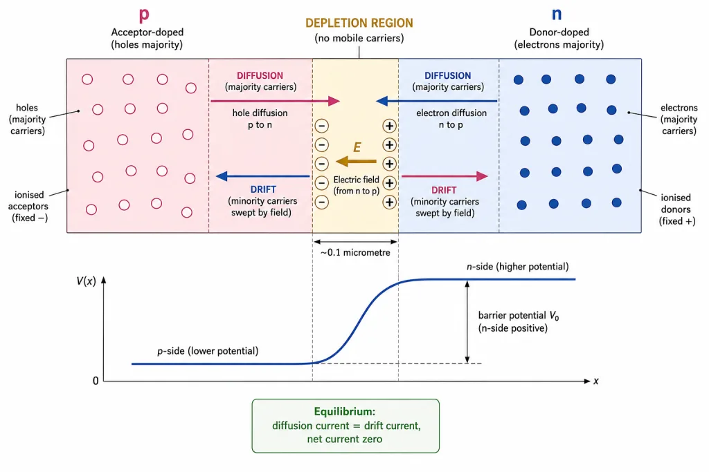
Diffusion vs Drift: The Two Competing Currents
Two processes govern junction formation:
1. Diffusion (concentration-driven)
Electrons are abundant on the n-side, holes on the p-side. Concentration gradients drive holes p → n and electrons n → p: the diffusion current (p → n direction conventionally).
2. The space-charge region builds
- Each electron leaving the n-side abandons an ionised donor (+) — immobile, locked in the lattice → a layer of positive space-charge on the n-side.
- Each hole leaving the p-side abandons an ionised acceptor (-) → a layer of negative space-charge on the p-side.
This double layer, emptied of free carriers, is the depletion region — thickness of order one-tenth of a micrometre (~0.1 m).
3. Drift (field-driven)
The space charge creates an electric field from n to p (positive → negative). This field sweeps any electron on the p-side to n, any hole on the n-side to p: the drift current, opposite in direction to diffusion.
Equilibrium
Initially diffusion is large and drift small. As diffusion proceeds, the space-charge widens, the field strengthens, drift grows — until diffusion current = drift current. The junction is formed; under equilibrium there is no net current.
Key Point: The loss of electrons from n and gain by p leaves n positive relative to p — a potential difference across the junction whose polarity opposes further carrier flow. This is the barrier potential (NCERT Fig. 14.11).
[NEET Important] Directions to lock in: diffusion = majority carriers crossing (holes p→n, electrons n→p); drift = minority carriers swept back by the field; field points n → p; n-side is the positive side of the barrier. [JEE Tip] Typical barrier values (for later circuit work): ~0.7 V for Si, ~0.2-0.3 V for Ge — the same numbers reappear as cut-in voltages.
Solved Examples
Example 1: Why pressing slabs together fails (NCERT Example 14.3)
Can a p-type slab be physically joined to an n-type slab to make a p-n junction?
Solution:
- No. Interatomic spacing is ~2-3 angstrom.
- Any slab surface, however polished, has roughness much larger than this.
- Continuous atomic-level contact is impossible; the interface behaves as a discontinuity for flowing carriers.
- Takeaway: junctions are grown inside one crystal (by converting part of a wafer through doping) — never assembled mechanically.
Example 2: Who moves in diffusion? [Board Conceptual]
During junction formation, which carriers diffuse, which way, and why?
Solution:
- Holes: p → n; electrons: n → p.
- Driver: concentration gradients — each species flows from where it is abundant to where it is scarce.
- These are majority carriers crossing over; their motion constitutes the diffusion current.
- Takeaway: diffusion is statistics, not fields — it would happen even with no charge on the carriers.
Example 3: The immobile charges [Board Conceptual]
Why does the depletion region carry net charge although it has almost no carriers?
Solution:
- Departing electrons leave ionised donors (+) on the n-side; departing holes leave ionised acceptors (-) on the p-side.
- These ions are bonded into the lattice — immobile.
- The region is depleted of FREE carriers but charged by FIXED ions: positive layer (n-side) facing negative layer (p-side).
- Takeaway: 'depletion' refers to mobile carriers only; the fixed space charge is the whole point — it generates the field and barrier.
Example 4: Direction of the built-in field [NEET Rapid]
State the direction of the depletion-region electric field and of the drift current it drives.
Solution:
- Field: from the positive space charge (n-side) toward the negative (p-side): n → p.
- Drift: the field pushes p-side electrons → n and n-side holes → p — i.e. minority carriers swept 'home'.
- Drift current direction (conventional): n → p… more precisely, opposite to the diffusion current.
- Takeaway: diffusion sends majority carriers OUT; drift sends minority carriers BACK. Balance = equilibrium.
Example 5: Why equilibrium is inevitable [Board Reasoning]
Explain why the diffusion process cannot continue indefinitely.
Solution:
- Every diffusing carrier adds to the space charge, widening the depletion region.
- Wider space charge → stronger field → larger drift current opposing diffusion.
- The process self-limits: growth continues until drift = diffusion, after which no net charge crosses.
- Takeaway: negative feedback builds the junction and then freezes it — equilibrium with zero net current but two equal, opposing currents still flowing.
Example 6: The barrier's polarity [NEET Conceptual]
Which side of an unbiased junction is at higher potential, and what does the barrier oppose?
Solution:
- The n-side lost electrons (and gained none back); the p-side gained electrons.
- So n is positive relative to p — the barrier potential .
- Its polarity opposes further diffusion of majority carriers (it would push holes back to p, electrons back to n).
- Takeaway: the junction erects exactly the wall needed to stop its own construction — 'barrier potential' is literal.
Example 7: Depletion width order of magnitude [Numerical]
The depletion region is ~0.1 m thick and the barrier ~0.7 V (Si). Estimate the electric field inside.
Solution:
- Field: .
- Compute: V/m.
- Takeaway: megavolt-per-metre fields live inside every diode — strong enough to sweep any minority carrier instantly, which is why drift needs no encouragement.
Example 8: What 'no net current' hides [Conceptual]
At equilibrium the junction carries zero net current. Does that mean nothing is moving?
Solution:
- No — two currents flow continuously: diffusion (majority carriers over the barrier) and drift (minority carriers swept down it).
- They are equal and opposite, cancelling exactly.
- Bias will later upset this balance: forward bias boosts diffusion; reverse bias exposes bare drift.
- Takeaway: equilibrium is a tug-of-war at stalemate, not an empty field — the whole diode story is about tilting this balance.
Example 9: Sequence the formation story [Board Ordering]
Arrange: (a) drift equals diffusion, (b) majority carriers diffuse across, (c) space-charge layers build, (d) field and drift current grow.
Solution:
- (b) concentration gradients drive majority-carrier diffusion.
- (c) departing carriers leave immobile ions — space-charge (depletion) layers form.
- (d) the growing space charge strengthens the field, increasing drift.
- (a) drift catches up to diffusion — equilibrium; junction formed.
- Takeaway: b → c → d → a; the four-step chain is a favourite Board sequencing question.
Example 10: Barrier height and doping [JEE Insight]
Qualitatively, how would heavier doping on both sides affect the barrier potential and depletion width?
Solution:
- Heavier doping → larger concentration gradients → more diffusion before balance → larger barrier potential .
- But denser dopant ions supply the needed space charge in a thinner layer → narrower depletion region.
- Takeaway: doping turns the barrier up and the width down — the extreme case (very heavy doping, very thin depletion) is exactly what makes a Zener diode's sharp breakdown possible (Section 7).