
About This Section
The rationalised NCERT trimmed Zener diodes, optoelectronic devices and logic gates from the Board text — but JEE Main and NEET syllabi retain them, and they appear nearly every year. Everything here is tagged accordingly: master it for competitive exams; treat it as enrichment for Boards.
The Zener Diode — [JEE/NEET Important]
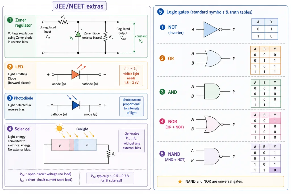
A Zener diode is a special diode designed to operate in the reverse breakdown region without damage:
- Heavily doped p and n sides → very thin depletion region (< m) → enormous junction field (~ V/m) even at small reverse voltages.
- Breakdown occurs at a sharp, well-defined Zener voltage ; beyond it, the voltage across the diode stays essentially constant at over a large current range.
- Symbol: diode with a bent (Z-shaped) bar.
Zener as a voltage regulator
Connect the Zener (reverse biased) across the load, fed through a series resistance :
- Input rises → extra current flows through the Zener, dropping the excess across ; load voltage stays at .
- Input falls (above ) → Zener current falls; load voltage still .
[JEE Tip] Regulator numericals are plug-ins of these two lines: find the series current, subtract the load current, check stays within ratings.
Optoelectronic Devices — [JEE/NEET Important]
Junction devices that couple photons and carriers:
LED (Light Emitting Diode)
- A heavily doped, forward-biased junction: injected minority carriers recombine radiatively near the junction, emitting photons with energy ≈ the band gap ().
- Visible LEDs need ≈ 1.8-3 eV (hence GaAsP alloys for red through yellow; GaAs itself, 1.4 eV, gives infrared).
- V-I like an ordinary diode but higher turn-on; advantages over incandescent lamps: low power, long life, fast switching, no warm-up.
Photodiode
- Operated in reverse bias with a transparent window; photons with generate electron-hole pairs in/near the depletion region, which the field separates → photocurrent.
- Photocurrent ∝ light intensity — measuring the easy-to-see change of a A-scale reverse current is why reverse bias is used (a A change atop A is detectable; atop forward mA it would drown).
- Uses: light detection, optical communication receivers.
Solar Cell
- A junction with a large exposed area, operated with NO external bias: photogenerated carriers are separated by the built-in field — electrons to n, holes to p — creating a photo-voltage.
- Delivers power to a load: characterised by open-circuit voltage and short-circuit current .
- Materials want ≈ 1.0-1.8 eV (Si 1.1 eV is ideal); criteria: good absorption, high conductivity, availability.
[NEET Important] Bias table: LED — forward; photodiode — reverse; solar cell — no bias. This three-way distinction is asked nearly every year.
Digital Electronics & Logic Gates — [JEE/NEET Important]
Digital circuits use only two voltage levels: 0 (low, 'false') and 1 (high, 'true'). A logic gate applies a Boolean rule to inputs A, B… producing output Y. The five gates:
NOT (inverter) —
| A | Y |
|---|---|
| 0 | 1 |
| 1 | 0 |
OR — (1 if ANY input is 1)
| A | B | Y |
|---|---|---|
| 0 | 0 | 0 |
| 0 | 1 | 1 |
| 1 | 0 | 1 |
| 1 | 1 | 1 |
AND — (1 only if ALL inputs are 1)
| A | B | Y |
|---|---|---|
| 0 | 0 | 0 |
| 0 | 1 | 0 |
| 1 | 0 | 0 |
| 1 | 1 | 1 |
NOR — (OR then NOT); NAND — (AND then NOT)
NOR: 1 only when both inputs are 0. NAND: 0 only when both inputs are 1.
Key Point: NAND and NOR are universal gates — each alone can build every other gate (e.g. NOT from NAND by tying inputs together; AND = NAND + NOT; OR from NANDs via De Morgan).
[JEE Tip] Waveform questions: convert the input timing diagrams to 0/1 intervals, apply the truth table interval by interval. Gate-identification questions: check the output at (0,0) and (1,1) first — those two rows distinguish all five gates instantly: (0,0)→1 means NOT-family (NOR gives 1, NAND gives 1); (1,1)→1 with (0,0)→0 means OR or AND — separated by the mixed rows.
Solved Examples
Example 1: Zener regulator basics [JEE Numerical]
A 6.0 V Zener regulates a supply varying from 10-16 V, through = 2 kohm, with no load. Find the Zener current range.
Solution:
- Series current (all through the Zener at no load): .
- At 10 V: mA. At 16 V: mA.
- Answer: 2-5 mA; the load would always see a steady 6.0 V.
- Takeaway: the Zener 'swallows' the input variation as current, dropping the excess volts across .
Example 2: Regulator with a load [JEE Numerical]
Same regulator ( = 6 V, = 2 kohm, = 16 V) now feeds a 3 kohm load. Find , and .
Solution:
- Series current: mA.
- Load current: mA.
- Zener current: mA.
- Takeaway: the junction rule at the Zener node — series current splits between load and Zener; the Zener takes whatever the load doesn't.
Example 3: LED colour from band gap [NEET Numerical]
An LED emits at 650 nm. Estimate the semiconductor's band gap.
Solution:
- Photon energy ≈ : .
- Compute: ≈ 1.9 eV — a red LED (GaAsP territory).
- Takeaway: (eV) = 1240/(nm); visible spans ~1.8 eV (red) to ~3.1 eV (violet) — hence the 1.8-3 eV LED-material window.
Example 4: Why photodiodes run in reverse bias [JEE Conceptual]
Justify operating a photodiode in reverse rather than forward bias.
Solution:
- Illumination adds a photocurrent of microampere scale (proportional to intensity).
- In reverse bias the dark current is itself only A — the photo-induced fractional change is large and easily measured.
- In forward bias the mA injection current would swamp the tiny photocurrent.
- Takeaway: detect small signals where the background is small — the measurement logic behind the bias choice.
Example 5: Solar cell vs photodiode [NEET Discriminator]
Contrast the two light-sensitive junctions in bias, purpose and output.
Solution:
- Photodiode: reverse biased; a detector — output is a current signal tracking intensity.
- Solar cell: no external bias; a power generator — the built-in field separates photo-carriers, producing and driving current through a load.
- Solar cells have large areas (collect maximum light); photodiodes are small and fast.
- Takeaway: same physics (photogeneration + field separation), opposite purposes — signal vs power.
Example 6: Identify the gate [JEE Pattern]
A two-input gate outputs 1 only when both inputs are 0. Name it and give its Boolean expression.
Solution:
- Check the signature row: (0,0) → 1, all other rows → 0.
- That is NOR: — OR followed by NOT.
- Takeaway: each gate has one signature row — NOR: only (0,0)→1; NAND: only (1,1)→0; AND: only (1,1)→1; OR: only (0,0)→0.
Example 7: NAND as universal gate [JEE Construction]
Build NOT, AND and OR using only NAND gates.
Solution:
- NOT: tie both NAND inputs together: .
- AND: NAND followed by the NAND-NOT: (two gates).
- OR: invert each input, then NAND them: (De Morgan; three gates).
- Takeaway: NAND alone rebuilds all logic — the meaning of 'universal gate' (NOR enjoys the same status).
Example 8: Waveform through a gate [JEE Waveform]
Inputs: A = 1 during t = 0-2 s and 4-6 s (else 0); B = 1 during t = 1-5 s. Sketch the AND output.
Solution:
- AND = 1 only when both are 1.
- Overlaps: A ∩ B = (1-2 s) and (4-5 s).
- Output: 1 in 1-2 s and 4-5 s, 0 elsewhere.
- Takeaway: intersect the high intervals for AND, union them for OR, complement for the N-gates — set language solves every waveform question.
Example 9: Cascaded gates [JEE Multi-step]
The output of an OR gate (inputs A, B) feeds one input of an AND gate whose other input is A. Simplify Y.
Solution:
- Expression: .
- Expand: .
- Answer: Y = A — the circuit ignores B entirely (the absorption law).
- Takeaway: simplify algebraically before tabulating; Boolean identities collapse many cascade questions to one letter.
Example 10: Choosing a solar-cell material [NEET Conceptual]
Why is silicon ( = 1.1 eV) preferred for solar cells over, say, a 3 eV material?
Solution:
- The solar spectrum peaks near ~1.5 eV photons; a cell converts photons with .
- ≈ 1.0-1.8 eV catches the bulk of solar photons; a 3 eV gap would reject most of the spectrum.
- Si adds practical virtues: good absorption, high carrier mobility/conductivity, and abundance.
- Takeaway: band gap must match the source spectrum — the same 1240/λ logic that painted the LED question, now run in reverse.